Showing posts with label circuit lab. Show all posts
Friday, 18 July 2014
Standard Resistor & Capacitor values - Table
By Unknown at Friday, July 18, 2014
circuit ideas, circuit lab, materials, Standard Resistor & Capacitor values - Table
29 comments
Friday, 11 April 2014
12V BATTERY HEALTH INDICATOR
By Unknown at Friday, April 11, 2014
12V BATTERY HEALTH INDICATOR, circuit ideas, circuit lab
No comments
This circuit is simple and easy to build & has only a few discrete components.
This indicates the 12V battery safe operating voltage.
Diode D1 protects the circuit when the battery polarity is reversed.
The LED glows with full brightness when the battery voltage is above the set threshold.
The threshold is set with the zener diode D2. for this circuit the threshold will
Vds+VBEq1 ~= 11.5V
When the Battery voltage is above 10.8V the LED glows with very little brightness & increases with increase in battery voltage.
When it is above 11.5V the LED glows with full brightness.
The resistance R1 limts the current flow through the LED, R2 limits base current.
The current consumption is very less. Approx 10mA for battery voltage above 13V & very lesser current consumption (in few uA) when battery voltage drops below 10.5V.
This indicates the 12V battery safe operating voltage.
Diode D1 protects the circuit when the battery polarity is reversed.
The LED glows with full brightness when the battery voltage is above the set threshold.
The threshold is set with the zener diode D2. for this circuit the threshold will
Vds+VBEq1 ~= 11.5V
When the Battery voltage is above 10.8V the LED glows with very little brightness & increases with increase in battery voltage.
When it is above 11.5V the LED glows with full brightness.
The resistance R1 limts the current flow through the LED, R2 limits base current.
The current consumption is very less. Approx 10mA for battery voltage above 13V & very lesser current consumption (in few uA) when battery voltage drops below 10.5V.
Wednesday, 9 April 2014
Rectangular Wave - PWM Waveform - Generation using 555
This simple circuit that produces a rectangular waveform using the most commonly available analog timer IC 555.
The on time and off time are controlled by the resistances Ra & Rb, which are variable to get the required value.
The formula for the time calculations are
The Circuit diagram is
The rectangular/pwm output is at pin 3 of the IC.
Resistance R1,R2 protects the device from shorting the terminals to VCC and ensure a minimum resistance available between the terminals.
The time delay depends on C2, RV1 & RV2. Change the values for desired output.
To get a square wave output, the condition is Ra=Rb. To get this, set the both pots to extreme left of right.
The on time and off time are controlled by the resistances Ra & Rb, which are variable to get the required value.
The formula for the time calculations are
The Circuit diagram is
The rectangular/pwm output is at pin 3 of the IC.
Resistance R1,R2 protects the device from shorting the terminals to VCC and ensure a minimum resistance available between the terminals.
The time delay depends on C2, RV1 & RV2. Change the values for desired output.
To get a square wave output, the condition is Ra=Rb. To get this, set the both pots to extreme left of right.
Saturday, 26 October 2013
About MAX7219 LED Display Dot-matrix Display Driver - Data Format - Register Map - Programming
By Unknown at Saturday, October 26, 2013
About MAX7219 display driver, circuit lab, embedded
2 comments
The
MAX7219 chip from maxim is a powerful serial input/output common-cathode
display driver that interfaces microcontroller to 7-segment numeric LED
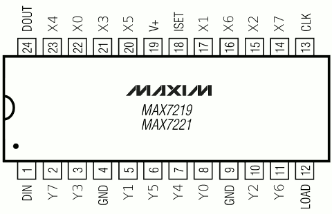
displays of up to 8 digits and a 8x8 dot-matrix displays. The pindiagram of MAX7219 is (for MAX7221, pin 12 is CS_bar)
Typical application circuit is
Many MAX7219 can be cascaded
serially through DOUT pin of one IC to DIN of the another, but with common
clock and load connections.
It needs only 3 wires to interface with the
microcontroller or microprocessor namely, CLK, LOAD and DIN. It has a build-in BCD (binary code decimal) decoder and a
brightness control. It is easy to enable or disable the BCD decoder through the
registers. Although the main function is to drive the 8-Digits seven segment
LED display but because it also capable to drive an individual LED segment i.e.
segment A to segment G and DP (decimal point), by disabling
the decoder.
The
MAX7219 chip has 16-bit registers divided into two ADDRESS and DATA each of 8 bit size. The data format for programming is
at the negative edge of CLK, the DIN appears at DOUT for cascading
In
order to send a command to the MAX7219 chip, first we need send the 8-bits
address and next we send the 8-bits data. It uses D8-D11 as address to map 14 registers. The register map is //
//Max7219 Command registers Address
DECODE 0x09 // Decode mode register Address
INTENSITY 0x0A // Intensity register Address
SCAN_LIMIT 0x0B // Scan limit register Address
SHUTDOWN 0x0C // Shutdown register Address
DISPLAY_TEST 0x0F // Display test" register Address
NOP 0x00
D0 0x01
D1 0x02
D2 0x03
D3 0x04
D4 0x05
D5 0x06
D6 0 x07
D7 0x08
//Max7219 Command registers Address
DECODE 0x09 // Decode mode register Address
INTENSITY 0x0A // Intensity register Address
SCAN_LIMIT 0x0B // Scan limit register Address
SHUTDOWN 0x0C // Shutdown register Address
DISPLAY_TEST 0x0F // Display test" register Address
NOP 0x00
D0 0x01
D1 0x02
D2 0x03
D3 0x04
D4 0x05
D5 0x06
D6 0 x07
D7 0x08
The data byte should be proceeded by the address byte.
The segment current is set by an external resistor (Rset) connected to pin 18 and VCC. The intensity can be controlled by software using Intensity register, setting values 1 (min) to 15 (max).
The Shutdown mode turns off all segment drives if its data is 0x00 and normal op if 0x01.
The Display test mode turns on all segment drives if its data is 0x01 and normal op if 0x00.
The Decode register is used to enable BCD decoder for the digits. the values are NONE=0x00, D0=0x01, D0-D3=0x0F, D0-D7=0xFF
The Scan limit register is used to set the number of used digits.
The
same principle is also apply to other important MAX7219 chip commands such as
activate from the shutdown mode (normal operation), use BCD decode (code B)
mode, scanning limit (scanning digit 0 to 7), and adjusting the seven segment
LED digit intensity please refer to the Maxim MAX7219 datasheet for the
complete explanation.
Comming soon: Interfacing MAX7219 with AVR for 7seg LEDs & later 8x8 dot matrix displays... Stay Tuned. Dont miss it.
This helps us to do much more better.
Monday, 7 January 2013
Elecdude Electronics Calculator for 555 calculations cd4060 CD 4011 -Capacitance code ,AC to DC calcuations
By Unknown at Monday, January 07, 2013
555 calculator, circuit ideas, circuit lab, ED Electronic Calculator, elec softwares, materials
1 comment
Elecdude Electronics Calculator
Here we give a simple electronics calculators for the followings. It is implemented in EXCEL & easy to use.
- 555 Astable multivibrator
- 555 Monostable multivibrator
- CD4060 Oscillator
- CD 4011 Oscillator
- Capacitance code calculator
- AC to DC calculations without transformer
If you have any doubt or issues in this, plz let us know.
We'll help you to overcome it.