• 1

    ..

  • 2

    ...

  • 3

    ...

Wednesday, 18 December 2013

DFT USING FFT MATLAB CODE - EXAMPLE


A fast Fourier transform (FFT) is an algorithm to compute the discrete Fourier transform (DFT) and its inverse. A Fourier transform converts time (or space) to frequency and vice versa; an FFT rapidly computes such transformations. As a result, fast Fourier transforms are widely used for many applications in engineering, science, and mathematics.

The FFT algorithm computes one cycle of the DFT and its inverse is one cycle of the DFT inverse. So it is the simple way to compute DFT of a sequence.


Here is a simple code to compute DFT of a sequence using FFT. The FFT is computed using the FFT(…..) function.

PROGRAM:
clc;
x=input('Enter the sequence : ');
n=input('Enter the length of FFT : ');

y=fft(x,n);
stem(y);
title('FFT');
xlabel('sample...');
ylabel('amplitude...');
disp('The FFT of the given sequence');
disp(y);
disp('The real value of FFT is ');
disp(real(y));
disp('The imaginary value of FFT is ');
disp(imag(y));
disp('The magnitude of FFT is ');
disp(abs(y));
disp('The phase of FFT is ');
disp(angle(y));
figure;
subplot(2,2,1);
stem(real(y));
title('Real');
xlabel('sample...');
ylabel('amplitude...');
subplot(2,2,2);
stem(imag(y));
title('Imaginary');
xlabel('sample...');
ylabel('amplitude...');
subplot(2,2,3);
stem(abs(y));
title('Magnitude plot');
xlabel('sample...');
ylabel('amplitude...');
subplot(2,2,4);
stem(angle(y));
title('Phase angle plot');
xlabel('sample...');
ylabel('amplitude...');
clear;

Input:
Enter the sequence : [2 4 6 8]
Enter the length of FFT : 5
Output:
The FFT of the given sequence
20.0000 ‐8.0902 ‐ 2.6287i 3.0902 ‐ 4.2533i 3.0902 + 4.2533i
‐8.0902 + 2.6287i


Waveform output:


If you enjoyed this post plz let us know your views via comments.
This helps us to do much more better.
Thankyou.


Sunday, 15 December 2013

Neyveli Lignite Corporation Limited (NLC) – Graduate Executive Trainee B.Tech/B.E

 Details of Post : Graduate  Executive Trainee

Neyveli Lignite Corporation Limited (NLC), a premier 'Navratna' Public Sector Enterprise with a present Annual Turnover of ` 5590 Crores (approx.) is spreading its wings in the frontiers of Mining and Power generation. The corporate plan of the company has many ambitious expansion schemes for capacity augmentation in the years to come. To add to its strength and fuel its growth, the company is looking for young, dynamic & result oriented talents for the post of Graduate Executive Trainee for its units and facilities located in various parts of the country (and abroad in future) through GATE 2014.

Educational Qualification  : B.Tech/B.E  or AMIE in respective Discipline

Discipline
Edu. Qualification
 (Degree or AMIE)
GATE 2014
Paper CODE
Mechanical
Mech
ME
Electrical
EEE
EE
ECE
EC
Mining
BE/B.Tech/B.Sc
MN
Control &
instrumentation
EIE/ICE
IN
Civil
Civil
CE
Computer
CE/CS/IS  or  PG degree in
Computer Applications
CS


  • Candidates with Degree in Electrical & Communication Engineering will have to appear for GATE- 2014 paper in EC code only although it is combined in Electrical Discipline as per NLC's requirement. Other than the above disciplines or combination degrees are not eligible.
  • Candidates should have passed qualifying degree in the above disciplines with 60% of marks for General & OBC and 50% for SC/ST.
  • Final year students may also apply however they should have obtained the Engineering Degree with the prescribed percentage of marks indicated above. In case of selection, they will have to submit their final mark sheet / provisional certificate by 31st August 2014.

IMPORTANT DATES: Online Submission of applications mentioning the GATE registration number in  NLC Website
20.12.2013 (10:00 hrs) to 20.01.2014 (17:00 hrs)


UPPER AGE LIMIT : Should not have completed 30 years as on 01.12.2013.

METHOD OF SELECTION : Eligible candidates will have to appear for GATE-2014. Candidates will be shortlisted based on Actual GATE-2014 Marks only (out of 100) for Group Discussion/Personal Interview. The list of candidates short listed for Group Discussion/Personal Interview will be available in our website www.nlcindia.com and also communicated to the candidates through e-mail.

COMPENSATION PACKAGE AND OTHER BENEFITS : Selected candidates will be offered attractive compensation package, approx Rs. 6.15 Lakhs CTC per annum, (which may be revised) and they will be on training for a period of minimum one year (extendable). During the training period the GETs will be paid Basic Pay, Dearness Allowance (presently 78.9 % of basic pay) and Common Allowance (40% of basic pay) per month. In addition to the above, they will be paid Performance Related Pay annually and entitled for superannuation benefit (30% of basic pay + Dearness Allowance), free Medical treatment for self and dependents; House Building Advance; Group Insurance; etc. as per rules. Eligible residential accommodation (unfurnished) will be provided depending on the place of posting at nominal rent.

PLACE OF POSTING : Selected candidates joining as GET in NLC are required to undergo training / work in any Unit / Area / Place situated in India and Abroad under the control of Neyveli Lignite Corporation Limited or in any Joint Venture / Associate / Subsidiary company of Neyveli Lignite Corporation Limited, to which they may be posted.

SERVICE & AGREEMENT BOND : Selected candidates while joining the post of Graduate Executive Trainee will be required to execute a Service Agreement Bond for a total value of Rs.1,00,000/- to serve the Corporation for a minimum period of three years after completion of training.

Mode of Payment of Application Fee:
     Payment of application fee could be made at any State Bank of India Branches (having core banking facility) using the Challan Form available on the Application Registration Portal. The Bank Challan printed from the portal only should be used for depositing the fee for proper crediting of amount in the allocated account. On receipt of the fee the concerned branch of SBI will issue a Unique Journal Number and a Branch Code of the branch collecting the fee. This journal Number and the Branch Code are to be filled up by the candidate during online registration.


Saturday, 14 December 2013

CHAINED IF COMPILATION IN AVR STUDIO - TIPS ON AVR PROGRAMMING


CHAINED IF COMPILATION IN AVR STUDIO
 

     Often chained if loop will be necessary for checking a port input status, but it may take up some unnecessary space & delay if not handled properly.

avr:elecdude

Thursday, 7 November 2013

MAX7219 7 Seg LED interfacing with AVR ATMEGA 8/16/32/328

        In previous post, we have seen in detail about MAX7219 & its registers and how to configure it. Now here we present an example of using MAX7219 with 7 segment LED interfacing with AVR ATmega family microcontroller.


LIST OF FUNCTIONS IN FOR  MAX7219  

  Shuts down or normals the Display (DON/DOFF)   MX7219_shutdown(sd)  
  Test the display or normal operation (NORM/TEST) MX7219_display_test(dt)
  Sets the Digit Brightness value (0x01 to 0x0F) MX7219_set_brightness(brightness)

  Set scan limit MX7219_set_scanupto(digit)

  Decode settings MX7219_set_decode(de)
        de -> NONE=0x00,  D0=0x01,  D0-D3=0x0F,  D0-D7=0xFF
  DECODE NONE MX7219_set_decode_NONE()

  Clear all 8 segments MX7219_clear_disp()
  Blanks all 8 segments MX7219_blank_bcd_disp()
  Display a BCD digit MX7219_dispbcd(pos,dat)
  Display a Matrix MX7219_disp_matrix(mat,size,st)
  Initialize 7219 MAX7219_init()


Here is the circuit diagram interfacing AVR ATmega8 with MAX7219 to 7 Seg LED


The Proteus simulation output for the project is shown below,


Click here to download the AVR Project file with C code & MAX7219 Header file.


If you enjoyed this post plz let us know your views via comments.
This helps us to do much more better.
Thankyou.

Saturday, 26 October 2013

About MAX7219 LED Display Dot-matrix Display Driver - Data Format - Register Map - Programming


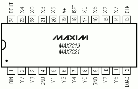
                The MAX7219 chip from maxim is a powerful serial input/output common-cathode display driver that interfaces microcontroller to 7-segment numeric LED displays of up to 8 digits and a 8x8 dot-matrix displays. The pindiagram of MAX7219 is (for MAX7221, pin 12 is CS_bar)

MAX7219
Typical application circuit is


Many MAX7219 can be cascaded serially through DOUT pin of one IC to DIN of the another, but with common clock and load connections. 

        It needs only 3 wires to interface with the microcontroller or microprocessor namely, CLK, LOAD and DIN. It has a build-in BCD (binary code decimal) decoder and a brightness control. It is easy to enable or disable the BCD decoder through the registers. Although the main function is to drive the 8-Digits seven segment LED display but because it also capable to drive an individual LED segment i.e. segment A to segment G and DP (decimal point), by disabling the decoder.

         The MAX7219 chip has 16-bit registers divided into two ADDRESS and DATA each of 8 bit size. The data format for programming is
at the negative edge of CLK, the DIN appears at DOUT for cascading

                In order to send a command to the MAX7219 chip, first we need send the 8-bits address and next we send the 8-bits data. It uses D8-D11 as address to map 14 registers. The register map is //               

           //Max7219 Command registers Address
               DECODE         0x09      // Decode mode register Address
               INTENSITY     0x0A      // Intensity register Address
               SCAN_LIMIT   0x0B      // Scan limit register Address
               SHUTDOWN   0x0C      // Shutdown register Address
               DISPLAY_TEST  0x0F     // Display test" register Address
               NOP  0x00
               D0  0x01
               D1  0x02
               D2  0x03
               D3  0x04
               D4  0x05
               D5  0x06
               D6  0 x07
               D7  0x08

          The data byte should be proceeded by the address byte.
       The segment current is set by an external resistor (Rset) connected to pin 18 and VCC. The intensity can be controlled by software using Intensity register, setting values 1 (min) to 15 (max).

          The Shutdown mode turns off all segment drives if its data is 0x00 and normal op if 0x01.

          The Display test mode turns on all segment drives if its data is 0x01 and normal op if 0x00.

        The Decode register is used to enable BCD decoder for the digits. the values are NONE=0x00,  D0=0x01,  D0-D3=0x0F,  D0-D7=0xFF

        The Scan limit register is used to set the number of used digits. 

      The same principle is also apply to other important MAX7219 chip commands such as activate from the shutdown mode (normal operation), use BCD decode (code B) mode, scanning limit (scanning digit 0 to 7), and adjusting the seven segment LED digit intensity please refer to the Maxim MAX7219 datasheet for the complete explanation.


          Comming soon: Interfacing MAX7219 with AVR for 7seg LEDs & later 8x8 dot matrix displays... Stay Tuned. Dont miss it.


If you have any doubts/need any clarification plz let us know your views via comments or mail us through   admin@elecdude.com
This helps us to do much more better.

Thankyou.

Search Here...